|
|
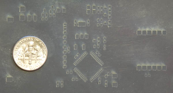
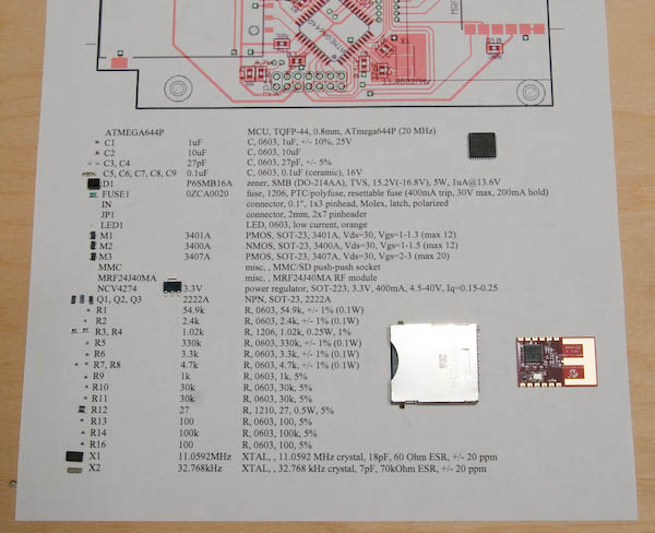
Using a Solder Stencilby Cathy Saxton I recently tried using a stencil for applying solder paste to a PCB's pads for surface-mount components. This page is a summary of what I learned. Thanks to Tom for all his time taking such excellent photos! Making the StencilI use EAGLE to design circuit boards. (I also have a page with tips for using EAGLE.) It automatically includes a 'cream' layer that can be used to create a stencil for applying solder paste to the pads for surface-mount components. (Just export using the CAM Processor, as you do when creating files to send to a board house for manufacturing.) The cream area is a property of each part, including being automatically created for SMD pads in library packages/devices that you create. LasercuttingI had Metrix Create:Space cut the stencil from a piece of 3 mil (0.003") mylar that I supplied. After some experiments, I decided to adjust the stencil cutouts generated by EAGLE. The laser cutter will actually make a hole a little larger than what's in the file, due to some combination of laser kerf and melting of the stencil material. In EAGLE, the cream area defined by a part is usually the same size as the SMD pad. Fortunately, it's possible to modify the cream layer on an entire board (as opposed to one part at a time), making the cream areas slightly smaller than the pads themselves. Here's how: From the board, open the DRC (Design Rule Check). Click on the Masks tab, and set the Cream Min and Max to 0.05mm (mm, not mil!). Click Apply. Your board's cream layers will be updated. Yes, this is surprising since it's labeled as a 'check' activity but does actually adjust the layers. You will, of course, need to do this for each board. A stencil, shown with a dime for scale: Stencil on the PCB, offset slightly (shifted down and to the right): Stencil in place on the PCB: Cutting with a Silhouette CameoIn December, 2011, I got a new toy: a cutting plotter! It's the Silhouette Cameo, and its software will cut any pattern I want (not just pre-fab "cartridge" designs). My page on the Cameo includes details on how to cut 3 mil mylar with the Cameo. The cuts are clean and precise, as good as or better than I've gotten with a lasercutter. Preparing to SolderFor complex and crowded boards, I use a cheat-sheet. It's got a list of all the components
as they are labeled on the board, and a picture of the board, including a bunch of documentation
references that aren't shown on the PCB. This lets me easily see the placement and orientation
for each component. I got all of the components that I needed to mount to the board and placed
them on the paper next to their labels. This made it pretty quick to place all the parts after
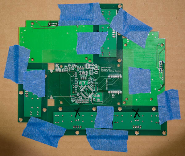
the solder paste was on the board. Mounting the StencilTo hold the board to which I wanted to apply solder paste, I put some scrap PCBs around it and
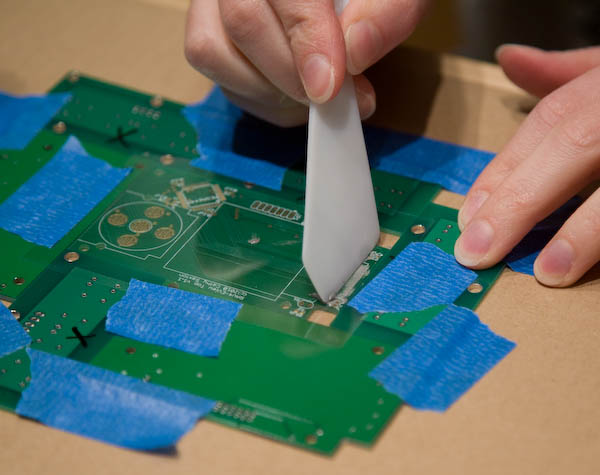
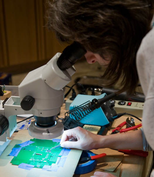
taped everything down with blue tape. I positioned the stencil and taped it on one side, checked
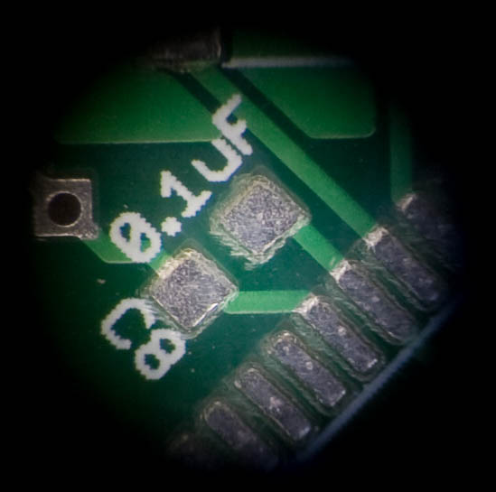
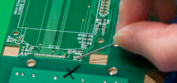
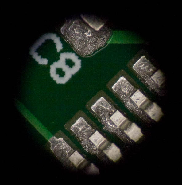
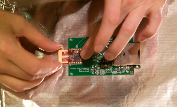
under the microscope, adjusted a bit, then taped the other 3 sides of the stencil. Close-up of stencil on PCB (taken through a microscope eyepiece).
Look at the edges of the pads for the edge of the mylar. Applying the Solder PasteI tried three different applicators. I'm pretty happy with the last one. The first time, I was using a fairly soft material for the squeegee and it tended to squish into the larger pads and dig out the paste that should have stayed there. After some back and forth trying to solve this, I peeled off the stencil, and as I feared, I'd managed to push some solder under the stencil between pads with close spacing. So, I scraped all the paste off the board and cleaned up the bottom of the stencil for round two... The second attempt went better. I used a stiffer -- but still slightly rubbery -- material. The edge probably wasn't as straight as would be ideal, so I still had some problems with the larger pads. Fortunately, the smaller pads turned out beautifully! The large pads were easy to touch up using a pin to apply a bit more solder paste. I had two issues with the second applicator: it seemed like it was still too soft, and ironically also had rough edges that scraped up the stencil.
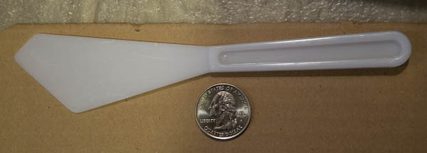
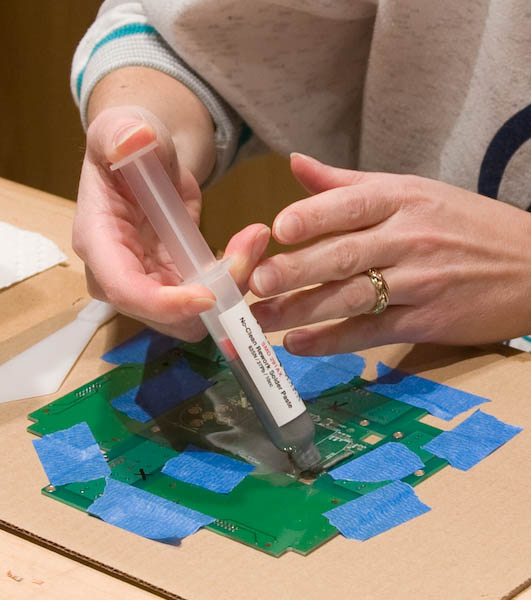
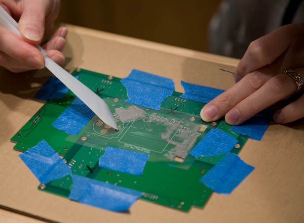
So, I went in search of something harder and less rough. I found a pack of various-shape plastic 'flexible palette knives' at Michaels. $1.99 for the set. Sold! I selected my favorite shape, sanded it lightly to remove a couple of burrs, then used 400-grit sandpaper and 0000 synthetic steel wool to ensure that its edge was nice and smooth. Application tool #3: Putting a strip of paste on the stencil: Smoothing solder paste over pads: I found that it worked well to apply a thick layer of paste over the microcontroller pads, then scrape most of the excess off. Trying to apply and remove in one pass resulted in some pads not getting any solder. Scraping off thoroughly to get the stencil completely 'clean' resulted in removing some paste from the pads. For the board here, the long edge of the knife worked well; I use the shorter edge for smaller boards.
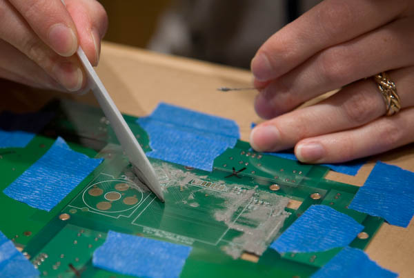
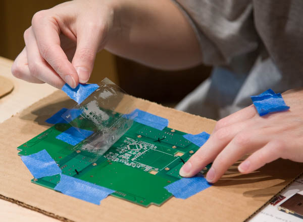
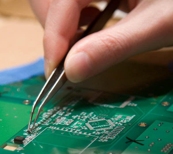
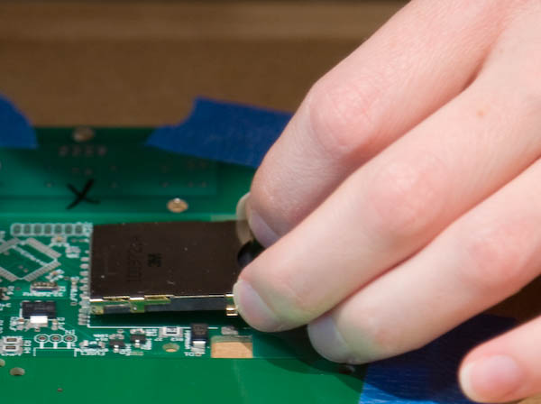
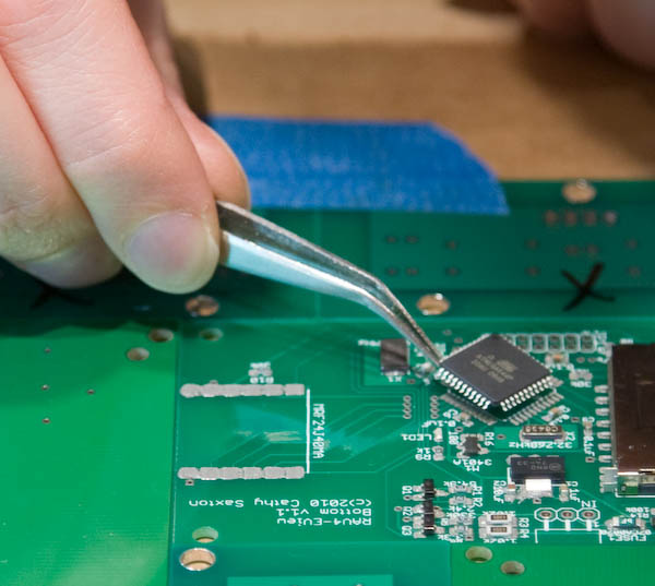
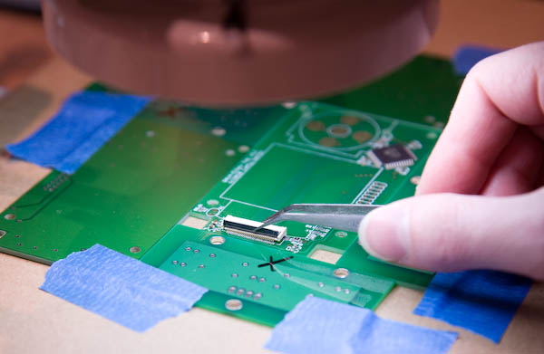
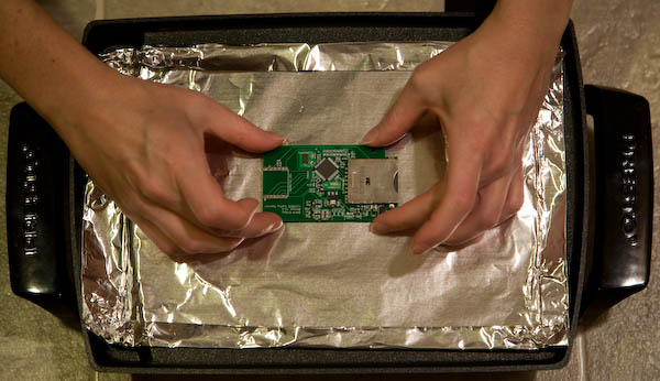
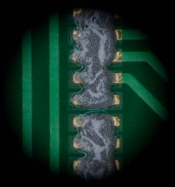
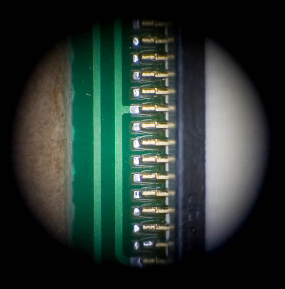
Applying a nice thick layer of paste over microcontroller pads: Scraping excess paste from the stencil: The above picture shows my original technique for removing excess paste. More recently, I've been holding the knife closer to horizontal with the excess paste on top, sort of like shoveling snow. Peeling off the stencil after applying paste: After removing the stencil from the board, I was able to clean off the bits of paste that were still on its surface, saving that paste in a small jar. I checked the board under a microscope, then touched up pads that I thought needed a bit more solder. With the second applicator, that included some larger pads that had lost solder as I'd scraped the stencil. For the third (good) applicator, I just needed to touch up a pad that I'd missed. Touchup on a section I missed: Placing ComponentsPlacing parts is the same as for boards pasted without a stencil: tweezers for small items and fingers for larger items. I tend to work my way from upper left to lower right, but place large items last. I placed the parts with the board still held in place by surrounding boards. After placing parts, I look at the board under a microscope and adjust as necessary. Placing a small part: Placing a large part: Placing a microcontroller: Adjusting microcontroller placement (possible without a scope, but easier with one): Close-up of paste with microcontroller placed: Very small components are easiest to place by viewing through a microscope. The most challenging part for this project is a connector with 30 pins that are each just 0.5mm apart. See below for photos of how this turned out! Placing connector (by viewing through a microscope): Heating the boardI've been using a griddle for soldering. It heats and cools quickly and has reasonably even heat over its surface. Details on that are on the Griddle Soldering page. After the components were placed, I carried the whole assembly over to the griddle. I carefully removed the tape securing the 'holding' boards, then placed my board on the griddle. This board has a part that overhangs the edge, so I decided to place that part after the board was on the griddle, just prior to turning on the heat. Putting board on griddle: Adding last component: Before heating: All done! After about five minutes: (note how the pasted areas go from dull gray to shiny silver) Examining one component closely, you can see how the heat first makes the solder paste expand a bit, then melts the solder, which tends to wick onto the pins and pads. Before heating, then after some warming when it starts to look worse! Probably the most dramatic example of this effect is evident by looking at the before and after photos of a 0.5mm-pitch connector. Close-up of paste on 0.5mm-pitch connector pads: Close-up of 0.5mm-pitch connector after soldering: |
| ©2000-2026 Idle Loop Software Design, LLC. You may not copy or reproduce any content from this site without our consent. |